Wacker Chemie AG (Munich, Germany) commissioned its new production line for the manufacture of ultra-pure semiconductor-grade polysilicon at its Burghausen production site in Germany. Accompanied by customers, suppliers and project partners, high-profile figures including Bavaria’s Minister-President Markus Söder and Gitta Connemann, Parliamentary State Secretary to the German Federal Ministry for Economic Affairs were among the guests who attended the official ceremony to mark the opening of the plant, called “the Etching Line Next.”
“Ultra-pure polycrystalline silicon is the purest man-made material. Everything regarding the semiconductor industry and, consequently, digital transformation revolves around this key raw material,” emphasized Wacker CEO Christian Hartel while addressing 100 guests in Burghausen, and added, “We are the only company in Europe and the largest in the world who manufactures ultrapure polysilicon for the semiconductor industry. The Etching Line Next allows us to further consolidate our position as a global quality and technology leader.”
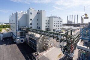
The new production line at Wacker’s Burghausen production site supplies hyperpure semiconductor-grade polysilicon for the microelectronics industry. (Photo: Wacker Chemie AG)
The internet, autonomous driving, Industry 4.0 – digital transformation and ever-growing data volumes in an ever-increasing number of data centers are driving the demand for polysilicon, one of the key raw materials in today’s digital era. Polysilicon in the highest grade of purity is indispensable for producing high-performance chips required, for example, in artificial intelligence applications or supercomputers. Very few companies are able to meet the more stringent purity requirements of the semiconductor industry. In the polysilicon business for over 70 years, chemical company WACKER is the world’s leading producer of this key raw material in the semiconductor industry.
By investing in a new production line for semiconductor-grade polysilicon, Wacker continues to expand its activities in this sector. Compared to 2024, the company aims to double its sales to semiconductor customers by 2030. “The new production line is a key project for our growth,” remarked Wacker CEO Christian Hartel, and elaborated further, “WACKER is a global leader in the semiconductor sector. Today, every second computer chip is made from polysilicon delivered by Wacker. Etching Line Next will not only allow us to meet the growing demands of the semiconductor industry, but also to achieve an exceptionally high product quality and a very high level of stability in production processes. Thanks to our new line, we can consistently produce polysilicon that will enable developers and manufacturers to come up with even more powerful logic and memory chips for the most demanding applications, such as artificial intelligence. In short: no polysilicon from WACKER, no AI.”
With a total expenditure of over €300 million, Etching Line Next is currently the Group’s largest investment project. Construction work began in fall 2022. Commissioning took place in stages from fall 2024. The plant recently went into operation and is already producing its first consignments. By virtue of the new production line, Wacker is increasing its production capacity for products that comply with the highest semiconductor-grade standards by more than 50 percent. This expansion in capacity will also create around 150 new jobs.
Cleaning the surface of the polysilicon chunks, which serve as a raw material for producing semiconductor wafers, is a complex and technically demanding process. Acids are used to remove the uppermost layer from the polysilicon surface. The chunks are then rinsed, packaged and shipped, whereby all operational steps are to a large extent automated and performed under cleanroom conditions. The ready-to-ship polysilicon now has a purity of over 99.9999999999%. The concentration of critical impurities is only in the parts-per-trillion range. This corresponds to not more than a grain of sugar in an Olympic-size swimming pool filled with water.
Important research and innovation projects were also initiated at the start of the project. An innovative cleaning process in conjunction with highly automated processes consistently guarantees the highest level of product purity. This enables WACKER to meet the growing quality demands that are essential to produce hyperpure silicon wafers and semiconductor chips.
Innovative technologies were also used during the planning phase. For example, production and logistics processes were planned virtually and simulated with the help of computer-aided simulation software. This resulted in significant cost savings and made it possible for the plant to be commissioned much earlier than the scheduled date.
As part of the European Union’s Important Projects of Common European Interest (IPCEI) program for microelectronics and communication technologies, funding of up to €46 million has been approved for research and innovation projects initiated by WACKER. The funding bodies include the German Federal Ministry for Economic Affairs and Energy, the Bavarian Ministry for Economic Affairs, Regional Development and Energy, and the European Union.